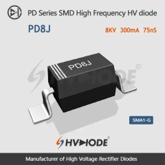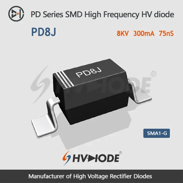
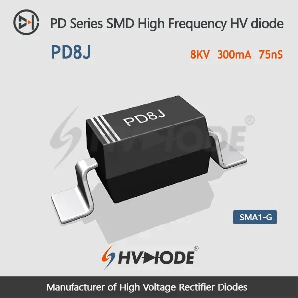
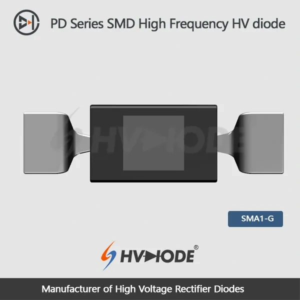
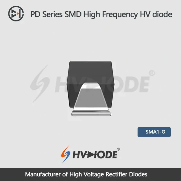
The PD8J is an SMD high voltage diode for boards that have to block 8 kV and still switch cleanly. It combines an 8 kV repetitive peak reverse voltage, a 300 mA average forward current and a 75 ns reverse recovery time in a compact gullwing-lead package, so it fits dense high-voltage layouts where a through-hole rectifier would not. Inside the PD series this part covers the 8 kV, 300 mA point: the same voltage class and the same body as the higher-current PD8M, but rated for stages that draw around 300 mA rather than 450 mA. That is useful when a board already carries a PD-series land pattern and the current requirement changes — the footprint, the reflow profile and the 75 ns switching behaviour stay exactly as they were. It is one part of a wider line that also covers fast recovery diode types in SMD and axial formats, power-frequency types for 50/60 Hz rectification, SiC high-voltage diodes, silicon stacks, rectifier bridges and complete high-voltage assemblies.
Eight kilovolts is the number that decides how many devices stand in a rectifier string. With an 8 kV repetitive peak reverse voltage and an 8 kV peak working reverse voltage, one SMD high voltage diode covers a large share of a medium-voltage secondary in an X-ray tank or an industrial supply. A shorter string means fewer solder joints in series, less total forward drop across the chain and a smaller board area given over to rectification.
The rating is quoted at 25 °C ambient with reverse current held to 1.0 µA, so it describes real blocking behaviour rather than a theoretical ceiling. Leave margin between your continuous rail and the working figure, and size the margin against the transients your topology actually produces rather than against a rule of thumb.
Forward conduction is rated at 300 mA average, measured on a 50 Hz half-sine wave into a resistive load at a 50 °C reference temperature. Treat that as the continuous figure to design the DC rail against. Short events are a different matter: the part absorbs a 10 A surge on a 0.01 s half-sine pulse, which covers the charging kick when a capacitor bank fills at power-on and usually removes the need for a separate inrush limiter.
Forward drop deserves as much attention as blocking. The forward peak voltage is 8.8 V or higher, far above the 0.7 V people carry over from low-voltage silicon, so the dissipation at 300 mA is set almost entirely by copper area, potting compound and any airflow in the enclosure. Plan the thermal path around that figure before the layout is frozen.
Where the 8 kV class earns its place: industrial power supplies rectifying a high-tension secondary, X-ray generator tanks, medical device supplies, and any bridge or voltage-doubler stage where a compact surface-mount high voltage rectifier has to hold off the full rail.
Surface-mount construction changes the assembly line as much as the circuit. There are no leads to form, no holes to drill and no hand-soldering step: the diode is placed by the pick-and-place machine and reflowed with the rest of the board, which keeps the high-voltage section on the same process as the low-voltage side instead of splitting the build into two routes.
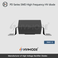
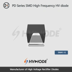
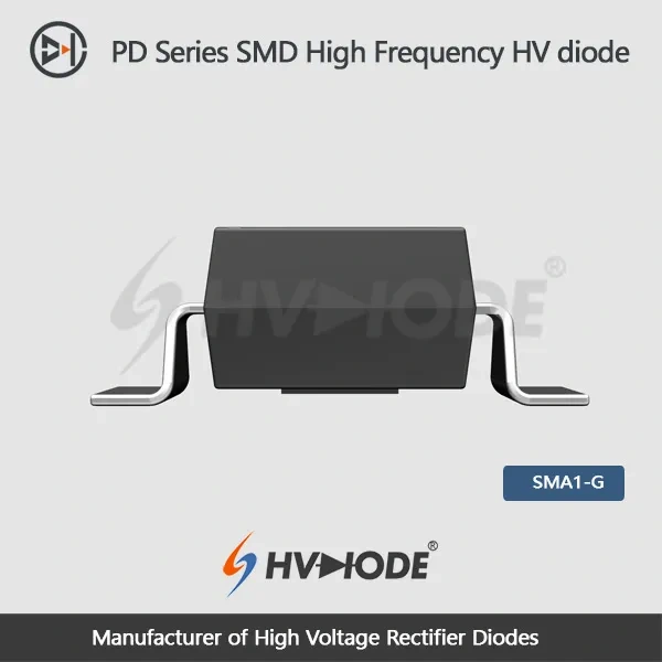
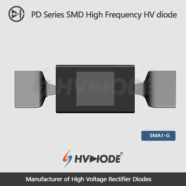
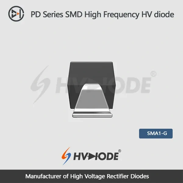
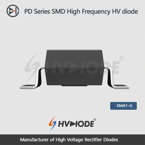
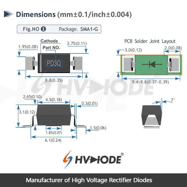
The gullwing, outer-bend terminals are the reason the joint is easy to trust. The lead foot rests flat on the pad and solder wicks up the heel and along the toe, so an inspection camera or a trained operator can confirm a fillet on both sides without turning the board over — a genuine advantage on a board that will later be potted.
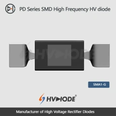
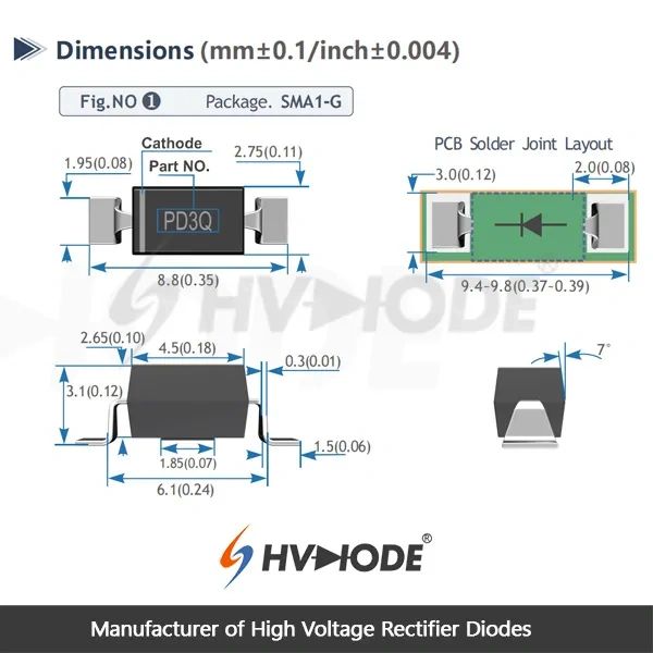
Because the body is small and flat, this SMD high voltage diode can sit in gaps that a larger axial part would force you to leave open. That matters in imaging boards where the high-voltage section is squeezed between a transformer, a multiplier and the output connector, and where every millimetre of creepage distance has already been accounted for.
The package is shared across the PD series, which means one land pattern and one stencil aperture set can serve several current ratings. If a design later moves from 300 mA to 450 mA, the board does not have to change and the qualification file does not have to be reopened.
Orientation is marked on the body: a white stripe identifies the cathode side and the part marking is printed on the black molding. Check the first article against the land pattern drawing before the run starts — a reversed high voltage rectifier in a series string usually fails destructively rather than simply underperforming.
A rectifier of this size is rarely used on its own, so it helps to see where it actually sits.
In an X-ray generator tank it works inside the high-tension multiplier, rectifying the secondary of the step-up transformer at the far end from the control electronics. Medical imaging supplies — DR panels, CT gantries, dental panoramic units — use it for the same job in a smaller enclosure, where a shallow surface-mount board has to fit inside a housing that was never designed around a through-hole stack. Industrial non-destructive testing sets and DC high-voltage generators use high voltage diodes of this class in the output rectifier, frequently in series strings where the 8 kV blocking voltage sets how many devices are needed.
On the switching side it appears in high-frequency inverters feeding a step-up transformer, in bridge rectifier stages after the transformer, and in fast-switching industrial controllers where recovery behaviour has to stay predictable across the operating range. Compact high-voltage modules and PCB assemblies use it when the whole multiplier has to be reflow-compatible and built in one pass.
| Repetitive peak reverse voltage (Vrrm) | 8 kV at Ta = 25 °C, Ir = 1.0 µA |
| Peak working reverse voltage (Vrwm) | 8 kV at Ta = 25 °C, Ir = 1.0 µA |
| Average forward current (If(AV)) | 300 mA, 50 Hz half-sine, resistive load, 50 °C reference |
| Reverse recovery time (Trr) | 75 ns |
| Surge forward current (Ifsm) | 10 A, 0.01 s half-sine, 50 Hz |
| Forward peak voltage (Vfm) | 8.8 V or higher |
| Reverse leakage at 25 °C (Irrm1) | 1.0 µA at VRM = VRRM |
| Reverse leakage at 100 °C (Irrm2) | 20.0 µA at VRM = VRRM |
| Operating ambient temperature (Ta) | −55 to +175 °C |
| Storage temperature (Tstg) | −55 to +150 °C |
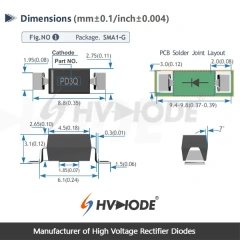
| Package | Surface mount, gullwing outer-bend leads |
| Mounting | Reflow soldering |
The quickest way to qualify a second source is to put the high voltage diode on your drawing side by side with the datasheet. Send the part number printed on the existing device, the datasheet if you still have it, and the column of values your drawing actually controls — repetitive reverse voltage, average forward current, surge current, recovery time, package outline and lead shape. We return the same six figures from our own data for the closest models and mark each one as an exact match or as a difference you have to accept or design around. Marking on the old body helps but does not settle it: house numbers and re-marked parts are common, so where the print is worn or unreadable, a photo of the package and the land pattern tells us more than the number does.
Inside the PD series the comparison is unusually clean because the body is shared. If your drawing asks for 8 kV at roughly 300 mA, the PD8J is that point; if the same drawing later asks for more current at the same 8 kV, the PD8M sits in the identical package at 450 mA, so pads and stencil stay as they are and only the thermal calculation needs revisiting. Where the original part was larger, compare the land pattern rather than the body outline — a smaller package that keeps the same terminal spacing can usually drop onto existing pads, while a different lead bend cannot. The same footprint logic runs through the PF series, which shares one package size across its 20 kV and 25 kV ratings, so a voltage step inside that family stays within a single land pattern.
Some substitutions should not be attempted. The 2CL types are axial-leaded power-frequency rectifiers built for 50/60 Hz duty and they carry no recovery-time figure, so they are not interchangeable with an SMD fast recovery diode on a switching rail even when the blocking voltage looks close — package, mounting method and intended duty all differ. Nor does a matching voltage number alone make two parts equivalent: a 5 kV, 800 mA device and an 8 kV, 300 mA device can both serve a high voltage rectifier stage, and the choice comes down to which margin your circuit is short of. Send the rail voltage, load current and switching frequency together with the old part number, and we will tell you which figure in your design the replacement has to preserve. Typical applications include high-frequency inverters, bridge rectifier circuits, and fast-switching industrial controllers where quick response is critical.
Selection starts with your circuit, not a catalogue number: tell us the working voltage, load current, switching frequency and ambient cooling conditions, and our engineers will match a model from our range and explain the margin left in the design. Each model ships with its datasheet, package drawing and installation guide, and we stay available for mounting and soldering questions, start-up checks and fault finding when an existing part runs hot or fails early. Orders run from about 7 days to 6 months depending on quantity, usually by international express.
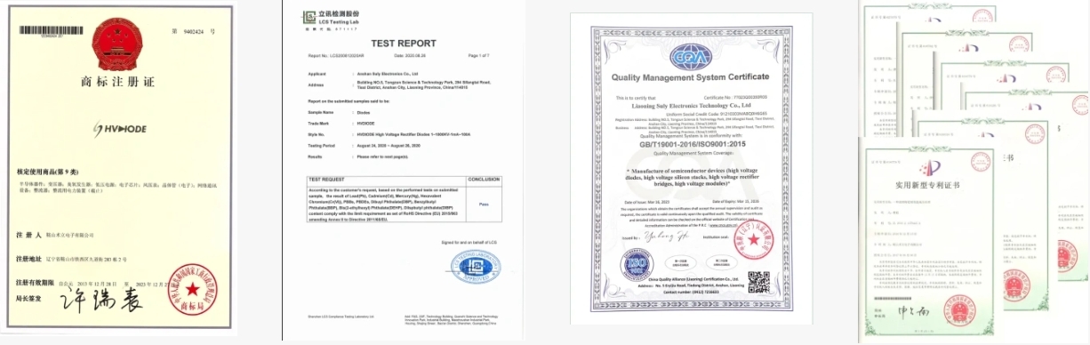
HVDIODE has manufactured semiconductor high-voltage rectifier components since 2008, and this diode comes off the same line and the same benches as the rest of that range. The company operates an ISO 9001 quality management system, and its materials and finished parts are covered by RoHS and SGS certification. Testing happens in house rather than being sampled from a catalogue. A multi-voltage-level high-voltage test bench checks blocking behaviour; a high-temperature and voltage-bias bench together with a high/low temperature chamber covers the temperature extremes; a leakage current tester and a TRR tester confirm the two figures that matter most on this part; and a surge impact bench plus a Vf/Vr parameter simulation bench check forward and reverse characteristics. The benches are calibrated against national metrology standards — the difference between a datasheet figure and a measured one. For a design engineer, that shows up as parameter spread you can plan around. Units drawn from different batches hold the same 8 kV blocking, the same 75 ns recovery and the same leakage class, so a design that passed qualification does not drift once it reaches volume production. It is also the reason buyers shortlist HVDIODE ahead of other high voltage diode manufacturers when a part has to hold its ratings under sustained thermal stress. The company runs its own R&D programme with universities and research institutes, holds patents on high-voltage component work, and supplies both research groups and production OEMs. Service follows the same pattern: where a standard part does not fit, customization of the diode and its assembly can be discussed against your specification, technical answers come from the people who build the parts, and a customer service contact stays with an order from enquiry through to delivery.