The PC5H is a surface-mount high voltage diode for rectifier and multiplier stages that stand off several kilovolts. It holds a 5 kV repetitive peak reverse voltage and the same 5 kV peak working reverse voltage, carries 200 mA of average forward current, and recovers in 75 ns — a set of ratings aimed at switching supplies rather than only at mains-frequency rectification. The body is a compact J-lead package with the terminals bent inward underneath, moulded in a high-thermal-conductivity epoxy that moves heat out of the chip and into the leads and copper. A cathode band and the printed model and rating stay readable before and after soldering, which matters when a board carries a column of identical parts. It is one step in the PC series of SMD high voltage diodes, a range that runs from 100 mA to 900 mA on a single package size. Typical homes are high-voltage rectifier strings, multiplier stages and bias or clamp positions inside imaging generators, non-destructive testing equipment and high-voltage test gear, where the diode sits on a PCB inside an oil tank, a gas-filled compartment or a potted module. - Surface-mount terminals — The part is reflow-soldered flat to the board, so it runs on the same automated line as the rest of the assembly with no drilling, lead forming or hand work. - High-thermal-conductivity epoxy molding — The mould compound carries heat from the chip to the leads and the copper beneath them, which is how a body this small holds a 200 mA average forward current at a 50 °C reference temperature. - 75 ns reverse recovery — Commutation losses stay small per switching cycle, so the diode belongs in switching rectifier positions and not only in slow, line-frequency ones. - J-lead, inner-bend terminals — The leads turn inward under the body, shortening the current path and tightening the outline; it also brings the two poles close together, which makes the surrounding medium part of the design. - Ultra-small outline — A small footprint leaves room in multiplier ladders, where several diodes stack in series and board area per stage is scarce. - One package size across the PC series — Every SMD high voltage diode in the family, from 100 mA to 900 mA, shares the same package outline, so the parts are interchangeable on a board and can be placed with the same tooling.
The family covers 5 kV in five forward-current steps — 100 mA, 200 mA, 300 mA, 500 mA and 900 mA — and every one of them is built on the same package size. The 200 mA version sits one step above the smallest: twice the average forward current of the 100 mA diode on an identical land pattern, which is usually the reason a design that was running the smaller part near its limit moves here.
Choosing between the steps is mostly a dissipation question. Forward peak voltage climbs as the current rating goes up — 4.2 V or more at this step, against 3.7 V for the 100 mA part — so a larger diode in the same footprint carries the load more easily but converts more of it into heat. Work out the average forward current in your own rectifier leg, add the ripple and inrush you expect, and keep margin: if your figure lands around 150 mA this part is comfortable, and if it lands close to 200 mA the 300 mA step is worth pricing alongside it.
There is a second reason to stay inside the family. The current ratings are quoted at a 50 °C reference, while the part is rated to a 175 °C ambient, so a stage that runs hot needs the current derated rather than simply read off the table. Prototyping one step and moving up after a thermal test is a normal route for these high voltage diodes, precisely because the pads never change.
| Parameter | Value |
|---|---|
| Repetitive peak reverse voltage (Vrrm) | 5 kV at Ta = 25 °C, Ir = 1.0 µA |
| Peak working reverse voltage (Vrwm) | 5 kV at Ta = 25 °C, Ir = 1.0 µA |
| Average forward current (If(AV)) | 200 mA, 50 Hz half-sine, resistive load, Tbreak = 50 °C |
| Reverse recovery time (Trr) | 75 ns |
| Surge forward current (Ifsm) | 10 A, 0.01 s, 50 Hz half-sine |
| Forward peak voltage (Vfm) | ≥ 4.2 V |
| Reverse leakage at 25 °C (Irrm1) | 1.0 µA at VRM = VRRM |
| Reverse leakage at 100 °C (Irrm2) | 20.0 µA at VRM = VRRM |
| Operating ambient temperature (Ta) | -55 °C to +175 °C |
| Storage temperature (Tstg) | -55 °C to +150 °C |
| Package | SMA1-J surface-mount, J-lead (inner bend) |
| Body marking | Model and rating printed on the body, cathode band at the cathode end |
Two leakage points, not one. The parameter table gives reverse leakage at two temperatures, both with the full 5 kV reverse voltage applied: 1.0 µA maximum at 25 °C and 20.0 µA maximum at 100 °C. The twentyfold rise between them is what makes thermal specification matter in a high-impedance stage. The room-temperature figure tells you the part is healthy; the 100 °C figure is the one that decides whether your multiplier or bleed chain holds its output once the assembly is warm.
Where it enters the error budget. Leakage is additive along a string. Five of these SMD high voltage diode positions, each at its published 100 °C limit, sum to 100 µA of reverse current before the stage delivers anything to the load. Put that next to the current your rectifier actually supplies: if leakage is a small fraction of it, the design is comfortable; if the two are the same order, the output will track temperature rather than sit still.
What it does to a bleed chain or a hold node. A bleed resistor network or a charge-hold node with megohm impedance converts reverse current directly into a voltage error, because that current has to flow through the node's own resistance. Work out the drop this leakage creates across the impedance you have, and compare it with the accuracy the circuit needs.
Guardband above 100 °C. The 100 °C point is the highest published leakage value, while the part is rated for ambient temperatures up to +175 °C. The upper limit tells you the part survives there, not what it leaks there. Set the margin from the 100 °C number, and if the assembly runs hotter, raise it with us before the error budget is frozen.
The axial range uses a different basis. The 2CL axial high voltage diodes are specified at Ir = 2.0 µA rather than 1.0 µA, so a leakage figure taken from one family cannot be set directly against the other. If you are weighing an SMD part against an axial part for the same node, bring both onto the same current basis first.
Measuring it on your own board. Apply the full working reverse voltage, hold the assembly at the temperature it really reaches, and let the reading settle before you record it. Surface contamination and humidity both add current and look exactly like diode leakage — clean and dry the board, guard the measurement, and compare the result against the 25 °C figure to separate a part issue from a board issue.
What to tell us. Send the reverse voltage, the impedance of the node the diode sits in, the highest temperature the assembly reaches and the error you can live with. We will say whether this 200 mA part stays inside that budget or whether another step in the series fits the circuit better.
| Material | Cured behaviour and where it suits |
| Silicone | Cures to a clear, elastic rubber that absorbs shock and withstands severe hot-cold cycling from -40 °C to 200 °C |
| Silicone, typical use | Open-air and vibration-exposed boards where flexibility matters more than a hard surface |
| Acrylic | Cures to a clear, hard coating with low moisture absorption and a short cure time |
| Acrylic, typical use | Board-level protection that needs wear resistance and insulation without a long cure cycle |
| Urethane | Cures to a clear, hard coating with high wear resistance and stable behaviour at low temperature |
| Urethane, typical use | Cold-running equipment; the same coating is the least tolerant of sustained high temperature |
| Epoxy | Cures rigid and usually opaque, with strong moisture, chemical and wear resistance and good dielectric properties |
| Epoxy, typical use | Humid, chemically aggressive or mechanically exposed assemblies that need a hard shell |
Selection starts with your circuit, not a catalogue number: tell us the working voltage, load current, switching frequency and ambient cooling conditions, and our engineers will match a model from our range and explain the margin left in the design. Each model ships with its datasheet, package drawing and installation guide, and we stay available for mounting and soldering questions, start-up checks and fault finding when an existing part runs hot or fails early. Orders run from about 7 days to 6 months depending on quantity, usually by international express.
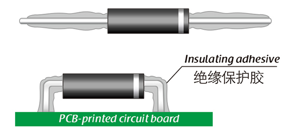
Here, suitable insulation adhesive materials can be selected based on the different usage situations of engineers.