Most high voltage diode manufacturers treat every current rating as a separate board design; the PC series is organised so the 300 mA step can be judged on current headroom and thermal margin rather than on a different circuit role. Use the printed part marking and cathode band to confirm the rating before assembly. If you are replacing an existing 5 kV SMD diode, compare Vrrm, Vrwm, If(AV), Trr, Vfm, the leakage limits at both temperatures, the terminal shape and the package outline. A part that matches voltage and current but uses a different lead bend may still need a land-pattern check. The 300 mA rating is the practical middle step: it gives more continuous-current headroom than the 200 mA part for a circuit that was running close to its limit, while avoiding the higher forward-voltage drop and thermal load of the 500 mA step. Do not choose a lower-current part just because it fits the outline; check worst-case load, surge and ambient. If the old marking is unreadable, send a clear photo of the board and the working conditions so the part can be compared with the PC series.
The PC5J is a 5 kV, 300 mA surface-mount high voltage diode with a 75 ns recovery time, built for high-voltage rectifier stages that need more current headroom than the lower steps in the PC series while staying inside the same compact SMD outline. Its molded epoxy body is chosen for high thermal conductivity, so heat from the chip has a short path into the board and surrounding insulation. The terminals use a J-Lead (inner-bend) shape for surface-mount soldering, and the package is deliberately small so it can sit close to multipliers, transformers and other high-voltage nodes. Fast recovery keeps switching losses low in high-frequency rectification. The part is supplied as a black molded SMD component with a cathode band and printed part marking for orientation and traceability.
| Parameter | Symbol | Test conditions | Value |
|---|---|---|---|
| Repetitive peak reverse voltage | Vrrm | Ta = 25 °C, Ir = 1.0 µA | 5 kV |
| Peak working reverse voltage | Vrwm | Ta = 25 °C, Ir = 1.0 µA | 5 kV |
| Average forward current | If(AV) | 50 Hz half-sine wave, resistive load, Tbreak = 50 °C | 300 mA |
| Reverse recovery time | Trr | — | 75 ns |
| Surge forward current | Ifsm | 0.01 s half-sine wave, 50 Hz | 10 A |
| Operating ambient temperature | Ta | — | -55 to +175 °C |
| Storage temperature | Tstg | — | -55 to +150 °C |
| Forward peak voltage | Vfm | — | ≥4.3 V |
| Reverse peak current at 25 °C | Irrm1 | Ta = 25 °C, VRM = VRRM | 1.0 µA |
| Reverse peak current at 100 °C | Irrm2 | Ta = 100 °C, VRM = VRRM | 20.0 µA |
Use the table as a design limit, not a typical value. The forward-voltage figure is a maximum, so conduction loss should be calculated from your actual current waveform, duty cycle and the copper area available to the SMD pads; at the 300 mA rating the part is intended for continuous load that is closer to the ceiling than the lower-current PC series steps, so leave thermal margin. The reverse-leakage table gives separate limits at room temperature and at 100 °C; a high-impedance bias or feedback node should be designed against the hot limit, because leakage climbs sharply with temperature. Recovery behaviour is fast enough for high-frequency rectification, but the layout still matters: keep the high-voltage loop short, respect creepage, and avoid running sensitive signal traces under the body. The surge rating is a short-pulse limit, not a continuous-current allowance, so check start-up inrush and capacitor-discharge events separately. The ambient and storage ranges are different; do not use the storage limit as an operating allowance. Finally, any insulating coating that improves the high-voltage surface margin also changes heat removal, so confirm the temperature rise with the coating in place.
Silicone. Silicone insulation adhesive usually cures to a transparent, elastic rubber. It absorbs shock and tolerates severe stress from large high-to-low temperature swings, including the -40 °C to 200 °C range called out for this material. Acrylic. Acrylic adhesives typically cure to a transparent, hard coating with low moisture absorption, fast curing, good wear resistance and good insulation. Urethane. Urethane usually cures transparent and hard, with superior wear resistance and good moisture resistance; it stays stable at low temperature but is less resistant to high temperature. Epoxy. Epoxy-based coating is very sturdy and usually opaque, with good moisture resistance, chemical resistance, wear resistance and dielectric properties. Choose by the insulation and thermal conductivity your design needs, the cure process your assembly can tolerate, and the service temperature at the diode. A coating that improves surface insulation can also trap heat, so match it to the temperature rise you measured rather than choosing on insulation alone. If you are unsure which material fits your potting or coating line, share the process conditions with us and we will help you compare the options.
Selection starts with your circuit, not a catalogue number: tell us the working voltage, load current, switching frequency and ambient cooling conditions, and our engineers will match a model from our range and explain the margin left in the design. Each model ships with its datasheet, package drawing and installation guide, and we stay available for mounting and soldering questions, start-up checks and fault finding when an existing part runs hot or fails early. Orders run from about 7 days to 6 months depending on quantity, usually by international express.
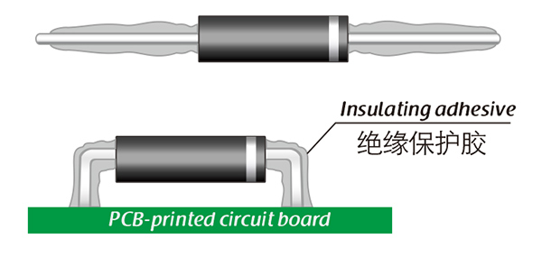
Here, suitable insulation adhesive materials can be selected based on the different usage situations of engineers.