• PC5S SMD high voltage diode 5KV,800mA,75nS
  • PC5S SMD high voltage diode 5KV,800mA,75nS
  • PC5S SMD high voltage diode 5KV,800mA,75nS
  • PC5S SMD high voltage diode 5KV,800mA,75nS
  • PC5S SMD high voltage diode 5KV,800mA,75nS
  • PC5S SMD high voltage diode 5KV,800mA,75nS
  • PC5S SMD high voltage diode 5KV,800mA,75nS
  • PC5S SMD high voltage diode 5KV,800mA,75nS
  • PC5S SMD high voltage diode 5KV,800mA,75nS
  • PC5S SMD high voltage diode 5KV,800mA,75nS

PC5S SMD high voltage diode 5KV,800mA,75nS

Products Main features:
1、SMD connection.
2、High thermal conductivity epoxy compound molding.
3、Fast recovery time for high efficiency.
4、J-Lead(Inner Bend) shapes.
5、Ultra small size package
6、Fast recovery PC Series are the same package size.
  • PC5S SMD high voltage diode 5KV,800mA,75nS
  • PC5S SMD high voltage diode 5KV,800mA,75nS
  • PC5S SMD high voltage diode 5KV,800mA,75nS
  • PC5S SMD high voltage diode 5KV,800mA,75nS
  • PC5S SMD high voltage diode 5KV,800mA,75nS
  • Desciption

  • data sheet

  • SMD HVdiode

  • Installation Guide

Product Overview

HVDIODE builds this part in its own plant in Anshan, and the same company produces the rectifier stacks and high-voltage assemblies these components end up in — useful when a 5 kV rating has to be checked against a real stack rather than a catalogue entry. The diode itself is a surface-mount rectifier for boards that must hold off several kilovolts in very little space. A moulded body, J-leads folded under the package and a fast-recovery junction let a high-voltage rail be rectified on the same PCB as the control electronics, instead of on a separate through-hole daughter board. Some arrive with a blank schematic and a new design; others are fitting a replacement into an existing board where the old axial part is no longer available or no longer fits. Day to day it behaves like any other surface-mount device: reel-fed placement, reflow alongside the rest of the board, then a high-voltage check at end of line. What differs is the layout discipline around it — pad spacing, board cleanliness and any coating decide whether a 5 kV design behaves; the package alone does not. Because these parts come directly from the high voltage diode manufacturers rather than through distribution, the drawing and the test data behind each rating can go straight to your design team.

Factory collage showing diode manufacturing, testing and bulk components.

SMA1-J Package & Footprint

  • J-lead, inner bend. The terminals fold under the moulded body instead of flaring outward, so the solder feet sit inside the package outline, the part stays compact and the joint keeps a little compliance when the board heats and cools.
  • Ultra-small moulded body. A flat black epoxy block with silver end terminals and a printed top marking; the cathode band shows the blocking end before the part reaches the nozzle.
  • Dimensioned drawing. The package drawing carries each dimension in millimetres with the inch equivalent and a ±0.1 mm (±0.004 in) tolerance. Work from that drawing rather than from a generic SMA land pattern.
  • PCB solder joint layout. A dedicated layout drawing gives the pad shapes and the spacing between them, which is the correct starting point for a 5 kV board.
  • Clearance around the part. Pad-to-pad gaps, slots and any coating are your design decisions; a clean, dry surface between the pads matters more at this voltage than the body size does.
  • Replacing axial parts. Compared with axial high voltage diodes, a surface-mount device removes lead forming and through-hole drilling and takes the height out of the assembly.
  • Placement. The flat top gives the placement nozzle a stable seat, and the body sits level on the paste — helpful on boards where a tilted part would change the clearance.
Close-up surface-mount rectifier diode labeled SMA1-J.

Industrial Automation

  • Power stages inside cabinets. Rectifying an internal high-voltage rail in inspection, test and role equipment, where the board has to stay small and the enclosure has no fan.
  • Sealed enclosures. A fast junction keeps switching loss per cycle low, which makes a closed box with no forced air a more realistic design.
  • Retrofit of older boards. Where high voltage diode manufacturers are phasing out an axial part, the surface-mount footprint gives back the height above the board for other components.
  • Continuous production lines. Standard SMT placement and reflow, so the rectifier does not need a separate assembly or soldering step on the line.
  • Field service. One part number per rail keeps the service kit small and the replacement procedure simple for a technician working inside a machine.
  • Short evaluation cycles. Engineers can test the part on an existing board instead of building a dedicated high-voltage fixture first.
  • Automated test equipment. Fast commutation suits the switching supplies that drive test and measurement heads, where a slow rectifier would blur the timing.

High Voltage Rectifier Systems

Inside a rectifier the diode is asked to do one thing well: conduct in one direction, block in the other, and get out of the way quickly when the polarity flips. This part sits in the high-voltage leg of that circuit, either on its own where the rail matches its class or as one element of a series string where the rail is higher.

Series operation is where most of the engineering effort goes. Each device in the string has to share the reverse voltage, and the division is set by leakage current, which moves with temperature — so strings are normally built with balancing resistors and checked hot as well as cold. Layout matters just as much: the spacing between devices, the coating over them and the cleanliness of the board all influence how the string behaves under load.

Around the string, the choices are conventional. A half-wave or bridge front end, a doubler where the transformer ratio allows it, a snubber where commutation is hard. What fast recovery adds is headroom — the rectifier can run at a higher frequency, so the transformer and reservoir capacitors can be smaller for the same ripple, and the high-voltage stage gets lighter overall.

Medical imaging and industrial X-ray supplies, non-destructive testing generators, electrostatic and high-voltage DC supplies, test transformers and radar power units all follow this pattern. If your rail is high enough that this high voltage diode would be one of several in series, tell us the string voltage and the number of devices and we will confirm the fit.

Recovery is the part of a rectifier's behaviour that shows up as heat rather than as output. While it conducts, charge builds in the junction of any high voltage diode; when the voltage reverses, that charge has to be swept out before the device blocks, and the current flowing during that window is pure loss. The 75 ns figure here is short enough that the loss per switching event stays modest even in the tens-of-kilohertz range where high-voltage supplies usually run. What that buys a designer is frequency headroom: for the same temperature rise the rectifier can switch faster, which lets the transformer and the reservoir capacitors in the high-voltage stage shrink. In a bridge or a voltage doubler it also sharpens the commutation, so snubber values and dead time can be tightened. Two practical notes. Recovery behaviour depends on how hard the part is driven — the applied dI/dt and the reverse voltage it is measured against both reshape the waveform, so verify the part in your own circuit rather than trusting a catalogue number alone. And this remains a fast-recovery silicon rectifier, not a zero-recovery device: for those 75 ns there is still reverse current, and a small RC snubber or a softer switching edge is often the cheapest way to keep the waveform clean when the commutating current is large.

High Current Rectification

Forward current is what separates this part from the rest of the surface-mount family. At 800 mA average forward current it can carry a rectifier leg on its own, so a design that would otherwise need two or three devices in parallel can use one — with one set of joints to inspect and one thermal path to manage. Current handling shows up in three places. In a charging or inrush stage the surge rating covers the short pulse while the average rating covers the steady state; keep the two apart, because a device that shrugs off the pulse can still cook on the average. In continuous rectification the practical limit is usually the solder joint and the copper around it, so give the pads and the trace real area instead of the minimum the layout drawing allows. And at these currents the forward drop dominates the loss, which means the copper carrying the current is also the heatsink. Check the number against your own duty cycle rather than the headline. If your waveform is far from sinusoidal, share it with our engineers and we will review the margin with you.

Datasheet Specifications

Repetitive peak reverse voltage (Vrrm)5 kV, Ta = 25 °C, Ir = 1.0 µA
Peak working reverse voltage (Vrwm)5 kV, Ta = 25 °C, Ir = 1.0 µA
Average forward current (If(AV))800 mA, 50 Hz half-sine, resistive load, Tbreak = 50 °C
Reverse recovery time (Trr)75 ns
Surge forward current (Ifsm)10 A, 0.01 s, 50 Hz half-sine
Forward peak voltage (Vfm)≥5.0 V
Reverse leakage at 25 °C (Irrm1)1.0 µA at Vrm = Vrrm
Reverse leakage at 100 °C (Irrm2)20.0 µA at Vrm = Vrrm
Operating ambient temperature (Ta)−55 to +175 °C
Storage temperature (Tstg)−55 to +150 °C
PackageSurface mount, SMA1-J, J-lead (inner bend)
SeriesPC series, common package size
Part numberPC5S

Thermal Path, Insulation & Durability

  • High thermal conductivity epoxy molding. The body is a moulded compound rather than a hollow case, so heat leaves the junction through the compound into the terminals and the copper beneath. On a dense board that path is often what keeps the junction inside its window without a heatsink.
  • Budget the forward loss. Use the datasheet forward voltage at your own peak current to estimate conduction loss, then treat the solder joint and the surrounding copper as the real limit — the ambient figure alone will not tell you whether the part runs cool.
  • Insulating adhesive over the chip. Before moulding, the junction area is covered with an insulating protective adhesive. That layer holds the high-voltage surface stable, keeps internal surface leakage low when the part is warm, and shields the chip from contamination working in along the lead frame.
  • Wide operating window. The ambient range runs from deep cold to well above any cabinet the part will live in, while storage is rated over a narrower band — worth knowing when stock sits in an unheated warehouse.
  • J-lead compliance. The bent lead absorbs part of the expansion difference between the moulded body and the FR-4 as the board cycles, which is what keeps the solder joint from becoming the wear item.
  • Durability over cycling. Repeated thermal cycling is normal life for this part; the joint, not the silicon, usually fails first, so first-article inspection and a look at joints after burn-in say more than a longer datasheet.
  • Handling. Keep parts in their original packaging until reflow, follow ESD precautions and avoid unnecessary reflow cycles — the moulded body is robust, but the chip and the joint are what care.

Future-Proofing & Cost of Ownership

Component cost is the smallest part of what a high-voltage board costs over its life. The expensive items are the redesign when a part disappears, the re-qualification when a package changes, and the field returns when a joint or a leakage path fails quietly months later. This part is chosen with those three in mind rather than with the unit price alone. Three things reduce the long-term bill. A shared package across the family means a voltage upgrade never touches the layout. A fast junction leaves thermal margin, so a later rise in switching frequency or cabinet temperature does not force a new board. And a documented part — datasheet, package drawing, PCB solder layout — lets the next engineer, or the contract manufacturer, pick it up without a phone call. Future-proofing also means planning the string rather than the single device. If the rail is expected to grow, lay out for the number of devices you will eventually need and populate only what the current design requires; the footprint cost is paid once. - One land pattern, several ratings. Every part in the PC series shares the same package size, so moving to a neighbour with a different voltage or current class does not reopen the layout or the stencil. - Growth by series connection. When the rail goes above what one device holds, add devices to the string; the footprint, the assembly drawing and the inspection procedure stay as they are. - Prototype to production. The part qualified on the bench is the part that runs on the line, with no package change between the two. - Assembly documentation. Each part number carries its own drawing and layout, so a contract manufacturer works from the number on the BOM rather than from a photograph of a previous build. - Service and rework. A single footprint across the family keeps rework stations, spare kits and training simple. - Working from the source. We are the high voltage diode manufacturers, not a reseller, so the drawings come from our own engineering team and a change of class can be confirmed against them before the BOM is released.

Installation & Soldering

  1. Check the printed marking and the cathode band against the silkscreen orientation before the reel goes onto the line.
  2. Compare the land pattern with the SMA1-J drawing, including the gap between the two pads, and confirm the stencil aperture matches the pad area you intend to use.
  3. Place the part with the rest of the surface-mount devices; the J-leads self-centre only slightly, so placement accuracy matters more here than on a gullwing part.
  4. Reflow to your solder paste supplier's profile. The moulded body takes standard lead-free reflow, but do not exceed the profile and do not run the part through more cycles than the process needs.
  5. Inspect the fillets under the body. At high voltage a void or a cold joint is the usual origin of a failure that only appears after weeks in the field.
  6. Clean the board thoroughly. Flux residue across a high-voltage gap is a leakage path, and the insulation inside the package cannot protect the board surface outside it.
  7. Test at your working voltage before coating, record the batch and the date code, and keep the result with the build record for traceability.

Ordering & Delivery

  • What to send. The part number, the quantity, and one line about the circuit — working voltage, load current and switching frequency — so we confirm the right element of the range before the order is released.
  • Presentation. Tell us whether your line needs tape and reel or whether bulk packing suits a rework bench; we will confirm what is available for your quantity.
  • Minimum order quantity and lead time. Both depend on the quantity band and current scheduling, so confirm them with your sales contact when you request the quotation.
  • Shipping. Orders ship by international express.
  • Payment terms. Confirmed with the quotation.
  • Documentation. Datasheet, package drawing, PCB solder joint layout and installation guide go with the order; tell us if your qualification file needs anything else.
  • Samples. Ask your sales contact about sample availability if the part has to be approved on a test board first.
  • Who answers. Your order is handled by the manufacturer's own sales and engineering team, so a question about a rating reaches the people who test it.

Technical Support & Model Matching

Each model ships with its datasheet, package drawing and installation guide, and we stay available for mounting and soldering questions, start-up checks and fault finding when an existing part runs hot or fails early. Orders run from about 7 days to 6 months depending on quantity, usually by international express.
FAQ

Will this part fit a board that was laid out for another diode in the PC series?

The PC series shares one package size, so the pads and the solder-joint layout carry across the family. The rating does not carry across: check the voltage class, the average forward current and the recovery time against your rail before swapping, and work from the drawing for the specific part number rather than a footprint downloaded for a neighbour. If you tell us which other high voltage diodes in the family you are comparing against, we will confirm the differences that affect your circuit.

How much margin should I keep below the reverse voltage rating?

The published figure is a limit measured under a defined condition, not a comfortable working point. Switching transients, surges coming in on the mains and the geometry of your own board all add to the voltage the device actually sees, so most designs run a single part well below its ceiling and put several in series where the rail is high, with balancing resistors across the string. Test the string hot as well as cold. Send us the waveform you expect across the device and we will tell you whether this high voltage diode is the right element for it.

Does reverse leakage change with temperature?

Yes, and the datasheet lists the leakage at two temperatures so you can plan for it. In a single device the change is small; in a series string it decides how the reverse voltage divides between the parts, which is why balancing resistors and a hot test are standard practice. If your string runs hot, go through the numbers with us before you fix the resistor values.

Is a 75 ns recovery fast enough for my switching frequency?

Recovery loss scales with the current being commutated and with how fast it is commutated, so frequency alone does not answer it. In a hard-switched converter running at tens of kilohertz, the 75 ns window is short enough that the loss stays modest. In a very fast circuit with a high dI/dt it can still dominate the switching loss, and a snubber or a softer edge is the better fix. Tell us the topology, the commutating current and the dI/dt you expect, and we will say where the part sits.

What package and lead form does it use?

It is a surface-mount part in the SMA1-J outline with J-leads that bend inward under the body. The body is a flat moulded block with terminals at the two ends and a printed marking on top, and the cathode end is indicated for orientation. A drawing dimensioned in millimetres and inches accompanies the datasheet, together with the recommended PCB solder joint layout.

Does the insulating adhesive replace conformal coating on the board?

No. The insulating adhesive sits inside the package and protects the chip and its junction area. The board surface around the part is still yours to manage: pad spacing, cleanliness and any coating you apply are what keep external leakage under control at high voltage. Treat internal insulation and board-level insulation as two separate jobs with two separate checks.

What documentation can I get for a design review?

The datasheet with the full ratings table, the package drawing, the PCB solder joint layout and the installation guide cover most reviews. If your qualification file needs something else, tell your sales contact what the document has to show and we will confirm what we can provide.

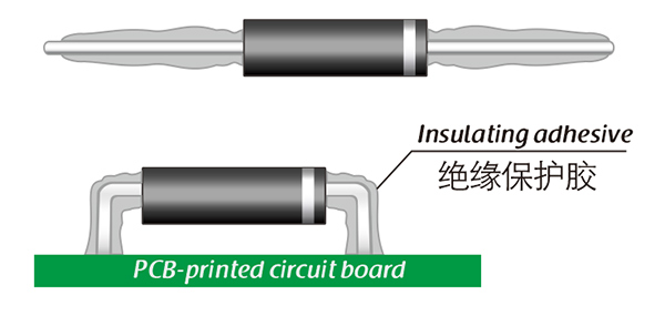
PC series SMD high voltage diodes, due to the design of inner bend angle.

During use, according to the actual working voltage level, it is necessary to pay attention to the insulation distance of the medium.

If it is used completely exposed to the air, it is recommended to fill the two poles with insulating materials, or immerse in three-proof paint, which will achieve more reliable insulation.

Of course, this will also affect the heat dissipation performance of the SMD high voltage diode.

Therefore, according to the temperature rise, there are different solutions for selecting insulating glue with suitable insulation and thermal conductivity.

Of course, this solution is not necessary, you just need to consider this aspect in your design plan.
In most cases, the working medium of insulating oil and insulating gas does not need to consider this kind of solution.
The selection of high-voltage diodes is closely related to their usage environment。

1. Used in insulating oil. (Recommended)
2. Used in insulating gases. (Recommended)
3. Secondary packaging use. (High requirements for heat dissipation and other parameter performance of components)
4. Use in exposed air or add air cooling. (If the size of the high-voltage diode is small, it is easy to discharge, and the heat dissipation performance is average.)

For high-voltage diodes used in exposed air, it is recommended to install them with insulated electrodes at both ends.


Common treatment methods for surface adhesive insulation:

Characteristics of insulation adhesive material:

1. Silicone material usually presents a transparent and elastic rubber state after curing, which is more effective in shock resistance and can also withstand severe stress changes caused by large high and low temperature changes (-40 ° C~200 ° C).

2. Acrylic materials typically exhibit a transparent and hard coating after curing, with low moisture absorption and fast curing time, as well as excellent wear resistance and insulation.

3. After curing, Urethane material usually presents a transparent and hard coating, which has superior wear resistance and good moisture resistance. Its performance is particularly stable in low temperature environments, but it is less resistant to high temperatures.

4. The coating material based on epoxy is very sturdy and usually opaque, with good moisture and moisture resistance. Its resistance to chemical corrosion and wear is also very good. In addition, epoxy also has good dielectric properties.

Here, suitable insulation adhesive materials can be selected based on the different usage situations of engineers.

HVDIODE - Suly Electronics Co., Ltd.

Expects To Provide You With Perfect Service

Name
Email *
Verification Code *
Click to verify
Leave a message
Name
Email *
Message
Verification Code *
Click to verify
We use Cookie to improve your online experience. By continuing browsing this website, we assume you agree our use of Cookie.