Product Overview
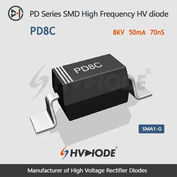
This is a surface-mount rectifier for the point where a high-voltage board has to get smaller and the diodes have to go on with the rest of the SMT line. It blocks the 8 kV class in a moulded epoxy body that is placed, reflowed and inspected like any other surface-mount component, so the multiplier no longer needs a through-hole footprint, formed leads and a hand-soldered joint.
That changes the layout as much as the process. Series stacks inside an X-ray tank board, a portable dental head or a non-destructive-testing supply can sit closer together, the assembly passes through the same reflow cycle as the rest of the board, and the current capability is an order of magnitude above the 5 mA axial parts in the same voltage class. Recovery is short enough that the diode does not set the ceiling on how hard the multiplier is driven.
It suits a design moving from wired axial rectifiers to board-level assembly, a compact head or probe with no room for leaded parts, or a surface-mount position that needs a higher blocking voltage than the part currently fitted.
As high voltage diode manufacturers, we list the full electrical set with the conditions each figure was measured under, so the part can be checked against an existing design on equal terms rather than on the headline voltage alone.
Assembly & Soldering
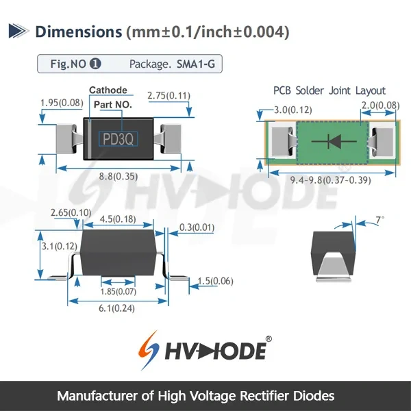
- The leads land outside the body, so a pattern copied from a leadless package will not fit.
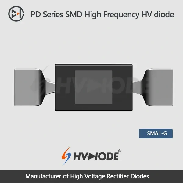
- Place with standard SMT equipment. Pick from the flat top of the moulded body and check orientation against the cathode band before the board enters the oven.
- Reflow on your existing profile. The body is moulded and the leads are ready for soldering; run the profile your board already uses, and check any preheat or bake step against the storage temperature on the data sheet.
- Inspect the fillet, not just the presence of solder. Look for a continuous fillet along the outer edge of every lead, with no bridging between adjacent pads; on a board carrying high voltage diodes a bridge is a short and a cold joint becomes a hot spot.
- Clean before you coat. Flux residue between pads forms a leakage path across the board surface. Clean and dry the assembly before conformal coating or potting so the coating bonds to a clean surface.
- Verify a first article. Check reverse blocking and forward drop on samples from the first board at the working voltage before the batch is released; a curve tracer or a leakage set shows a damaged part immediately.
- Rework with heat, not force. Preheat the board and lift the part with hot air. The outer bend of the lead is the weakest point mechanically, and levering the body off takes the pads with it.
Package & Board Fit
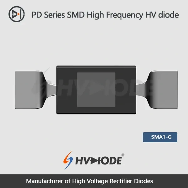
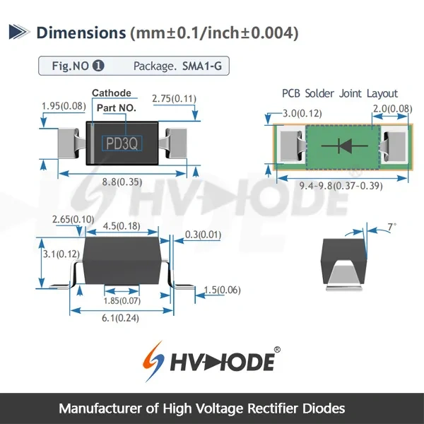
- Gull-wing, outer-bend leads. The leads are formed outward and sit flat on the land pads, so reflow produces a fillet along the outer edge that can be checked under a microscope or by AOI without lifting the part.
- Ultra-small moulded body. Compact size matters most in a string where several surface-mount high voltage diodes sit in series: every millimetre taken off the body is a millimetre left for the gap between high-voltage nodes.
- High thermal conductivity epoxy moulding. The chip is encapsulated in a moulding compound that both insulates the junction and gives heat a defined path out through the body and the copper under the leads.
- Cathode band on the body. A printed stripe identifies the cathode end. Check orientation against the silkscreen before the reflow pass — in a series string, one reversed part blocks the whole chain.
- Shared package with the PF series. The fast-recovery PF series uses the same package size, so a board laid out for this footprint can take a PF-series part without changing the stencil or the land pattern if the design later moves to a different rating in the family.
- Land pattern from the drawing. Take pad length, pad width and the gap between pads from the package drawing and the PCB solder joint layout supplied with your quotation. Because the leads bend outward, the pads run away from the body rather than under it.
- Copper as part of the heat path. The leads sit on copper, so the pad area beneath each lead carries heat away from the body. On a board that runs warm, keep that copper generous instead of minimum width.
Circuit Applications
- X-ray generator and DR/CT tank boards. The rectifier sits in the high-voltage multiplier inside the tank, usually in oil, and has to hold its blocking voltage while the tank warms up. A surface-mount body keeps the multiplier board small enough to fit the tank envelope.
- Portable dental panoramic heads. Head volume and weight are the binding constraints, and a reflowed board with no leaded rectifiers saves both, with no hand-soldered joint to fatigue under vibration.
- Non-destructive testing supplies. Portable X-ray inspection units run the same multiplier topology at lower power; a surface-mount high voltage diode lets the whole board be cleaned and potted as one unit.
- DC high-voltage generators and HVDC supplies. Series strings of rectifiers build the DC output, and a defined recovery time with a low forward drop keeps the stack efficient at the frequency the converter runs at.
- High-voltage test sets and test transformers. When the set has to be carried to the equipment, a board-level multiplier is easier to package, screen and shield than a wired rectifier assembly.
- Radar, accelerator and detector bias supplies. These need a bias rail that stays put as the enclosure heats, which is where a rectifier with controlled leakage at temperature earns its place.
Electrical Specifications
| Parameter | Rating and test conditions |
|---|
| Repetitive peak backward voltage, Vrrm | 8 kV at Ta = 25 °C, Ir = 1.0 µA |
| Peak working backward voltage, Vrwm | 8 kV at Ta = 25 °C, Ir = 1.0 µA |
| Average forward current, If(AV) | 50 mA, 50 Hz half-sine wave, resistive load, Tbreak = 50 °C |
| Backward recovery time, Trr | 70 nS |
| Surge forward current, Ifsm | 10 A, 0.01 s half-sine wave at 50 Hz |
| Forward peak voltage, Vfm | ≥8.0 V |
| Backward peak current, Irrm1 | 1.0 µA at Ta = 25 °C, VRM = VRRM |
| Backward peak current, Irrm2 | 20.0 µA at Ta = 100 °C, VRM = VRRM |
| Operating ambient temperature, Ta | -55 °C to +175 °C |
| Storage temperature, Tstg | -55 °C to +150 °C |
| Package | Surface-mount, gull-wing (outer bend) leads, ultra-small body |
| Encapsulation | High thermal conductivity epoxy compound moulding |
Thermal Design Checks
- Put the leakage budget on the hot figure. The data sheet gives reverse current at room temperature and again at 100 °C. The second figure is what a warm multiplier actually sees, so size the divider, the feedback network and any leakage-sensitive node around it rather than around the cold value.
- Treat the forward figure as a floor. Forward peak voltage is published as a minimum, not a typical, so allow the full value in your drive headroom instead of borrowing an average curve from another vendor's part.
- Measure the ambient where the diode sits. The operating ceiling is high, but the part usually lives beside the transformer or the multiplier stack. A thermocouple on the board during a soak run tells you more than the enclosure's rated ambient.
- Check process temperatures against the storage rating. The storage window is narrower than the operating window, so a bake, a hot cure or a long preheat before reflow should be checked against the storage figure, not the operating one.
- Match parts when you stack them. Several surface-mount high voltage diodes in series divide the reverse voltage according to their leakage. Keep a stack to one production lot, or fit grading resistors across each device, so no single part carries more than its share.
- Plan for the surge you can really get. The surge rating is quoted for a 0.01 s half-sine at 50 Hz. A flashover or an arc in a tank delivers a different shape, so add series impedance or a clamp wherever the load can arc.
Family Comparison & Creepage
Within the same 8 kV blocking class, the difference between this part and the axial 2CL71 is current capability and thermal headroom, not the voltage figure. Both hold 8 kV, and both recover in tens of nanoseconds — 70 nS here against 80 nS on the leaded part — so a low-current multiplier sees almost the same switching behaviour from either. The gap opens on the current side: 50 mA average forward current against 5 mA, 10 A of surge current against 0.5 A, and a forward peak voltage of ≥8.0 V against ≥23.0 V, which is less than half the conduction drop per device in a series string. The operating ceiling is also 25 °C higher, at +175 °C against +150 °C. Reverse leakage is the one figure that converges: 1.0 µA here at Ta = 25 °C against 2.0 µA, but both are quoted at 20 µA at Ta = 100 °C, so a hot stack does not share voltage any better just because the cold leakage figure looks tighter.
The choice between them comes down to how the board is built. The 2CL71 is an axial high voltage diode: its leads are formed, spaced and soldered one at a time, and lead length itself becomes part of the insulation gap between devices, which is why wired multipliers still use it. This part is placed and reflowed with the rest of the board, with the lead form and the land pattern taking over that job. Voltage class still deserves a deliberate decision rather than the highest number available — inside the axial family, the 6 kV 2CL70 and the 4 kV 2CL69 keep the 5 mA current and 80 nS recovery and bring the forward peak voltage down to ≥18.0 V and ≥16.0 V, so a multiplier that never passes 4 kV or 6 kV gains nothing from the 8 kV step.
The 2CL2P and 2CL2R answer a different requirement. Their 30 kV / 150 mA and 35 kV / 100 mA ratings are built for 50/60 Hz rectification in DC high-voltage generators, hipot sets and test transformers, and no recovery time is published for them because conduction lasts most of each half cycle. In a switching multiplier that figure is exactly what you need, so these two belong to mains-frequency supplies and should not be pulled in just to reach a higher blocking voltage. Even inside that pair the trade runs against the headline number: the 30 kV 2CL2P carries 50 mA more average current and 15 A of surge against 10 A on the 35 kV part.
None of this shortens the insulation distances your layout has to keep. Clearance and creepage are set by the copper and the board surface — the pads, the copper spreading under each lead, the gap to the next device in a string of high voltage diodes and the gap to any other high-voltage node — not by how small the moulded body is. An ultra-small package lets a longer series string fit into a given area, and that saved area is better spent on more distance between high-voltage nodes rather than taken back out of it. Keep the surface between and around the pads clean and dry before coating, and make sure the coating covers the whole leakage path, because the body insulates itself and nothing beside it.
Ordering & Delivery
If the design is being converted from a leaded rectifier, include the original part number and the footprint it used — the change of package is the step that catches people out. The data sheet, package drawing and PCB solder joint layout travel with the reply. As high voltage diode manufacturers we work from the specification you send rather than from a catalogue line, which is also how we handle a cross-reference: give us the original part's blocking voltage, average current, recovery time and forward drop, and we will show where this part sits against them and whether a different voltage step in the range is the closer match. Orders ship by international express. Quantity, packing, lead time and payment terms are confirmed with your sales contact for each order, because they depend on the voltage class, the quantity and the destination. Ask your sales contact about sample availability and current terms if you need them for a qualification build.
Technical Support & Model Matching
Selection starts with your circuit, not a catalogue number: tell us the working voltage, load current, switching frequency and ambient cooling conditions, and our engineers will match a model from our range and explain the margin left in the design. Each model ships with its datasheet, package drawing and installation guide, and we stay available for mounting and soldering questions, start-up checks and fault finding when an existing part runs hot or fails early. Orders run from about 7 days to 6 months depending on quantity, usually by international express.
FAQ
How does this compare with an axial 2CL diode at the same blocking voltage?
The voltage class is the same, but the two are built for different assembly routes. This is a surface-mount part with gull-wing leads: it goes through reflow with the rest of the board and takes a fraction of the footprint a leaded rectifier needs. It also carries a much higher average forward current than the 5 mA axial parts and is rated for a higher operating temperature. Choose the leaded version when the board is through-hole and lead length is part of the layout; choose this high voltage diode when the multiplier itself is a surface-mount assembly.
Can it be driven above 50/60 Hz?
Yes. The recovery time is short enough for a switching multiplier, which is where this part separates itself from a power-frequency rectifier. One thing to keep in mind: the published average forward current is measured on a 50 Hz half-sine into a resistive load, and at higher switching frequencies the conduction angle and the switching loss change the thermal picture. Send us the waveform and the frequency you intend to run and we will confirm the current the part can carry in your circuit.
Can it be used inside a potted or oil-filled assembly?
Yes, and that is one of the common ways it is used: the multiplier board is cleaned, coated or potted and then fitted into an oil-filled tank. The moulded epoxy body is an insulator in its own right, but the encapsulant has to bond to it and to the board around it, so check your potting compound against an epoxy-moulded body and make sure the assembly is dry and free of flux before coating. Once potted, the compound becomes part of the insulation path, so its dielectric behaviour matters as much as the diode's.
Can it serve as a second source for a part already on our BOM?
It can, as long as the electrical class and the package both line up. Send the original part number with its blocking voltage, average current, recovery time and forward drop, plus the land pattern on the board; we will show where this part sits against those figures and whether another voltage step in the range is the closer match. As high voltage diode manufacturers we compare against the specification you send rather than against a part number alone, which is what makes a cross-reference worth having.
Does the small body reduce the clearance I need on the board?
No. Clearance and creepage are set by the board layout, not by the component body. The body is compact, but the pads, the copper under the leads and the distance to the next part define the path across the surface. Keep the spacing your design rules call for, treat the area between pads as a leakage surface that has to stay clean, and make sure any coating covers it fully.