
Categories
  • PF25H SMD high voltage diode 25KV, 200mA, 75nS
  • PF25H SMD high voltage diode 25KV, 200mA, 75nS
  • PF25H SMD high voltage diode 25KV, 200mA, 75nS
  • PF25H SMD high voltage diode 25KV, 200mA, 75nS
  • PF25H SMD high voltage diode 25KV, 200mA, 75nS
  • PF25H SMD high voltage diode 25KV, 200mA, 75nS
  • PF25H SMD high voltage diode 25KV, 200mA, 75nS
  • PF25H SMD high voltage diode 25KV, 200mA, 75nS

PF25H SMD high voltage diode 25KV, 200mA, 75nS

Products Main features:
1、SMD connection.
2、High thermal conductivity epoxy compound molding.
3、Fast recovery time for high efficiency.
4、Gullwing(Outer Bend) shapes.
5、Ultra small size package
6、Fast recovery PF Series are the same package size.
  • Description

  • data sheet

  • Installation Guide

Product Overview

This part is a surface-mount high voltage diode for rectifier stages where the reverse voltage runs into tens of kilovolts but the board has no room for an axial component. It is rated at a repetitive peak reverse voltage of 25 kV and an average forward current of 200 mA, and it recovers in 75 ns — a combination that lets a compact switching supply hold off a very high reverse voltage without paying a large switching-loss penalty.

Physically, this SMD high voltage diode is a small black moulded block with gullwing leads bent outward at each end, a white stripe marking the cathode and the model code printed on the top face. Inside, a high thermal conductivity epoxy compound encapsulates the die and carries heat into the leads and the board, which is what supports an operating range of -40 to +175 °C in a package this size.

The design belongs to the PF family of fast recovery high voltage diodes, and every PF part shares the same package size. That consistency is used deliberately: a 15 kV, 20 kV or 25 kV build can be laid out on one footprint, and raising the voltage rating later does not mean redesigning the pads or the insulation geometry around them.

Typical service is inside the high-voltage section of medical imaging generators, industrial NDT and HVDC equipment, high-voltage test sets and radar power supplies, rectifying a high-frequency waveform ahead of the output filter. Because it is a bare component rather than a potted assembly, how you insulate it — oil, gas, potting compound or air — matters as much as the ratings on the datasheet, and the sections below deal with that directly.

Key Features

  • Surface-mount connection — the leads sit flat on the pads and solder in a reflow pass, so there is no through-hole drilling and no hand-wiring in the high-voltage section; the joint is also repeatable enough for automated assembly.
  • High thermal conductivity epoxy moulding — the encapsulant is chosen to move heat out of the die rather than trap it, which is what makes the -40 to +175 °C range usable when the part sits close to transformers and other heat sources.
  • 75 ns backward recovery — coming out of conduction in 75 ns keeps commutation loss small in switching supplies, which is why a fast recovery diode of this type is specified at high switching frequencies rather than line frequency.
  • Gullwing (outer bend) leads — the feet bend outward, giving a compliant joint that absorbs the expansion difference between the moulding and the PCB and lets an inspector see a fillet on all sides.
  • Compact body — the package keeps the high-voltage section short, and every millimetre of creepage path you do not have to engineer is worth having; a smaller SMD high voltage diode also leaves more room for the insulation around it.
  • One package across the PF series — 15 kV, 20 kV and 25 kV PF parts share the same outline, so a design can be uprated without touching the pad layout, the stencil or the tooling.

Model Selection

Two numbers decide most of these choices — the two that high voltage diode manufacturers put at the top of every datasheet: how much reverse voltage the circuit must hold off, and how much average current flows while it does. This model answers both at 25 kV and 200 mA, with a forward peak voltage of at least 16.7 V and 75 ns recovery — the higher-current half of the 25 kV pair in the PF family. The other half is the PF25F. It shares the 25 kV rating, the 75 ns recovery, the -40 to +175 °C range and the same package, but it is specified at 100 mA average forward current with a forward peak voltage of at least 15.6 V. Where the load current stays below roughly half of the 200 mA figure, the PF25F delivers the same voltage capability with a slightly lower forward drop. Where the current approaches or passes 100 mA, the extra headroom here is what keeps the die temperature honest, and it is the reason to choose this rating rather than the lighter one. If the design does not actually need 25 kV, stepping down buys current. The PF20J, for example, is rated at 20 kV and 300 mA in the same fast recovery diode family, so a rail working between roughly 15 kV and 18 kV can be rectified with more current margin and the same footprint and insulation geometry. The trade is straightforward: voltage margin above the working level, or current headroom through the part. Two practical notes before you commit a board. The 25 kV rating is a repetitive peak value measured at 25 °C with 1.0 µA leakage, so leave design margin for switching transients and for the leakage rise at elevated temperature. And check the current against the way the part will be cooled, because the 200 mA figure is quoted for a 50 Hz half-sine resistive load with the case at 50 °C — a potted or air-cooled build will not reach the same number without a temperature check.

Specifications

ParameterValue
Repetitive peak reverse voltage (Vrrm)25 kV at Ta = 25 °C, Ir = 1.0 µA
Peak working reverse voltage (Vrwm)25 kV at Ta = 25 °C, Ir = 1.0 µA
Average forward current (If(AV))200 mA, 50 Hz half-sine, resistive load, Tbreak = 50 °C
Backward recovery time (Trr)75 ns
Surge forward current (Ifsm)10 A, 0.01 s half-sine, 50 Hz
Forward peak voltage (Vfm)≥ 16.7 V
Reverse leakage at 25 °C (Irrm1)1.0 µA at VRM = VRRM
Reverse leakage at 100 °C (Irrm2)20.0 µA at VRM = VRRM
Operating ambient temperature (Ta)-40 to +175 °C
Storage temperature (Tstg)-40 to +150 °C
PackageSurface mount, gullwing (outer bend) leads
EncapsulationHigh thermal conductivity epoxy compound

Installation & Operating Environment

  1. Start with the insulation environment, because it sets the thermal and voltage conditions for everything else. Insulating oil is the recommended option for high-voltage duty, and insulating gas is the other recommended one; both suppress discharge and hold a stable dielectric around the moulding.
  2. If the board is potted or given a secondary package, work out the heat path before the compound goes in. A secondary-packaged diode places higher demands on heat dissipation and on the other parameters, so the compound, the copper area and the cure schedule have to be chosen together.
  3. Treat open air as the least forgiving case. A small body discharges more easily in air and the heat dissipation is only average, so add air cooling and keep a high voltage diode clear of sharp edges, bare high-voltage nodes and anything that collects dust.
  4. For any part mounted in exposed air, fit insulated electrodes at both ends. That is the usual way to keep the field away from the lead terminations, and it costs far less than a redesign once tracking appears.
  5. Seat the gullwing feet flat on the pads exactly as the package drawing shows. On assemblies that carry several high voltage diodes, a foot lifted off its pad concentrates the field at that point and opens a leakage path.
  6. Solder with a reflow profile that suits the board and the parts around it, and keep flux and residues off the body — contamination on a high-voltage surface is a tracking path waiting to happen.
  7. After cleaning, and again after potting or impregnation, run a leakage and withstand check. The insulation work is then verified rather than assumed, and a weak joint is caught before the assembly is sealed.

Insulation Adhesive Materials

  • Silicone — cures to a clear, elastic rubber that cushions the component against shock and absorbs the stress of large temperature swings; the cured material withstands the strain of -40 °C to 200 °C cycling, well beyond the diode's own range.
  • Acrylic — cures to a clear, hard coating with low moisture absorption and a fast cure, adding good wear resistance and insulation to the surface it covers.
  • Urethane — also cures clear and hard, with strong wear and moisture resistance and unusually stable behaviour at low temperature; of the four it is the least tolerant of sustained heat.
  • Epoxy — rigid and usually opaque once cured, with good resistance to moisture, chemical attack and wear plus solid dielectric properties; it is the choice when mechanical robustness matters more than seeing the joint afterwards.
  • Matching the compound to the assembly — a potted or oil-filled build can take a rigid epoxy, while a high voltage diode that will see repeated thermal cycling is usually better served by silicone's elasticity. Check dielectric strength and cure schedule against your own withstand test before committing a production batch.

Ordering & Delivery

  1. Send the model designation, the quantity and the working voltage, current and switching frequency of your circuit. The ratings are checked against the application before an order is released, because a part that looks right on paper can still be wrong for the way it is cooled.
  2. Ask your sales contact to confirm minimum order quantity, price and lead time for the quantity you need. As high voltage diode manufacturers we quote these per order rather than fixing them in advance, and a list mixing several PF voltage ratings can be handled in the same enquiry.
  3. Agree the shipping arrangement when the order is placed. International express is the channel used for these components, so confirm the delivery address and any paperwork you need travelling with the goods at that point.
  4. Request the datasheet, package size drawing and installation guide for the exact rating you have chosen if they are needed for an internal approval file. They set out the test conditions a design review will ask about, and the same documents cover the other high voltage diodes in the PF series.
  5. Re-check the part against the insulation method you will use before it ships. Oil, gas, potting and open air each change the thermal and voltage picture, and settling that before dispatch is far cheaper than discovering it after the assemblies are potted.

Technical Support & Model Matching

Selection starts with your circuit, not a catalogue number: tell us the working voltage, load current, switching frequency and ambient cooling conditions, and our engineers will match a model from our range and explain the margin left in the design. Each model ships with its datasheet, package drawing and installation guide, and we stay available for mounting and soldering questions, start-up checks and fault finding when an existing part runs hot or fails early. Orders run from about 7 days to 6 months depending on quantity, usually by international express.
FAQ

How is the cathode marked on the body?

A white stripe runs across one end of the black moulding, and the model code is printed on the top face. The stripe marks the cathode, so match it to the pad your layout designates as cathode before soldering. The marking is small and disappears under a coat of potting compound, so confirm the orientation before the assembly is sealed rather than afterwards.

How much voltage margin should I leave above the 25 kV rating?

Treat 25 kV as the repetitive peak reverse voltage the part is qualified to hold at 25 °C with 1.0 µA leakage, not as a level to run at continuously. Switching transients, load behaviour and the reverse leakage that climbs from 1.0 µA at 25 °C to 20.0 µA at 100 °C all stack on top of the steady-state voltage. Most designs will want headroom above the working level, and the amount depends on the waveform — send it to us and we will say whether the rating leaves enough room or whether the insulation and cooling need more attention instead.

Can this diode replace the part number printed on an older assembly?

Start from the code printed on the old body and its original datasheet rather than from the outline. Two parts can share the same package and still differ by a factor of two or three in average forward current, which only shows up as heat after the swap. Compare repetitive peak reverse voltage, average forward current, recovery time, forward peak voltage and the temperature range against this model; if you send a clear photo of the marking together with the old datasheet, we will tell you whether this rating is a safe replacement or whether another PF part is the closer match.

What does the forward peak voltage mean for heat?

The forward peak voltage is at least 16.7 V, so at the full 200 mA average current a meaningful share of the loss budget turns into heat inside the moulding. That heat leaves through the leads and the pads, which is why copper area, potting compound and local airflow all change how close the part runs to its -40 to +175 °C limit. On a tight board or in still air, measure the case temperature rather than relying on the headline current rating.

When would the HV37 series suit better than the PF series?

The HV37 range covers 6 kV to 15 kV with higher current ratings — up to 500 mA in air on the 6 kV part — but its operating range stops at 125 °C rather than the 175 °C of this family. If your rail sits below about 15 kV and current is the harder constraint, the HV37 series is worth a look. If you need 25 kV, or you need to keep running hot, stay in the PF fast recovery diode family.

The selection of high-voltage diodes is closely related to their usage environment。

1. Used in insulating oil. (Recommended)
2. Used in insulating gases. (Recommended)
3. Secondary packaging use. (High requirements for heat dissipation and other parameter performance of components)
4. Use in exposed air or add air cooling. (If the size of the high-voltage diode is small, it is easy to discharge, and the heat dissipation performance is average.)

For high-voltage diodes used in exposed air, it is recommended to install them with insulated electrodes at both ends.


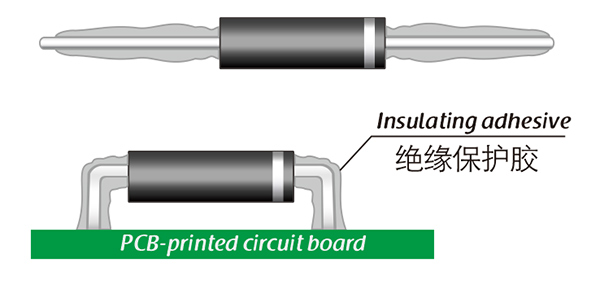
Common treatment methods for surface adhesive insulation:

Characteristics of insulation adhesive material:

1. Silicone material usually presents a transparent and elastic rubber state after curing, which is more effective in shock resistance and can also withstand severe stress changes caused by large high and low temperature changes (-40 ° C~200 ° C).

2. Acrylic materials typically exhibit a transparent and hard coating after curing, with low moisture absorption and fast curing time, as well as excellent wear resistance and insulation.

3. After curing, Urethane material usually presents a transparent and hard coating, which has superior wear resistance and good moisture resistance. Its performance is particularly stable in low temperature environments, but it is less resistant to high temperatures.

4. The coating material based on epoxy is very sturdy and usually opaque, with good moisture and moisture resistance. Its resistance to chemical corrosion and wear is also very good. In addition, epoxy also has good dielectric properties.

Here, suitable insulation adhesive materials can be selected based on the different usage situations of engineers.

  • PF25H SMD high voltage diode 25KV, 200mA, 75nS
  • PF25H SMD high voltage diode 25KV, 200mA, 75nS
  • PF25H SMD high voltage diode 25KV, 200mA, 75nS
  • PF25H SMD high voltage diode 25KV, 200mA, 75nS
Leave a message
Name
Email *
Message
Verification Code *
Click to verify
We use Cookie to improve your online experience. By continuing browsing this website, we assume you agree our use of Cookie.